This module is licensed under the MIT License
TODO
- Schematic
- Build prototype
- PCB Design
Introduction
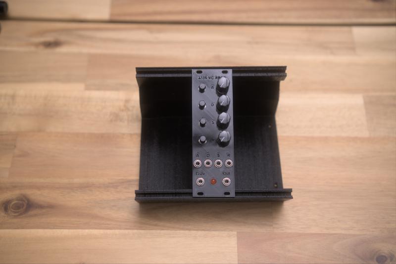
This module is a simple VC ADSR design. The design is based on the chip’s datasheet info.
Module Images

Demo
Module Features
Each envelope parameter is CV controllable (Attack, Decay, Sustain, Release)
I/O and Controls
Inputs:
- Gate input (0-5v, 0-10v)
- Attack CV input (10vpp)
- Decay CV input (10vpp)
- Sustain CV input (10vpp)
- Release CV input (10vpp)
Output:
- Envelope output (0-5v)
Controls (knobs):
Attack input attenuation knob
Attack offset knob (serves as control knob when no input is connected)
Decay input attenuation knob
Decay offset knob (serves as control knob when no input is connected)
Sustain input attenuation knob
Sustain offset knob (serves as control knob when no input is connected)
Release input attenuation knob
Release offset knob (serves as control knob when no input is connected)
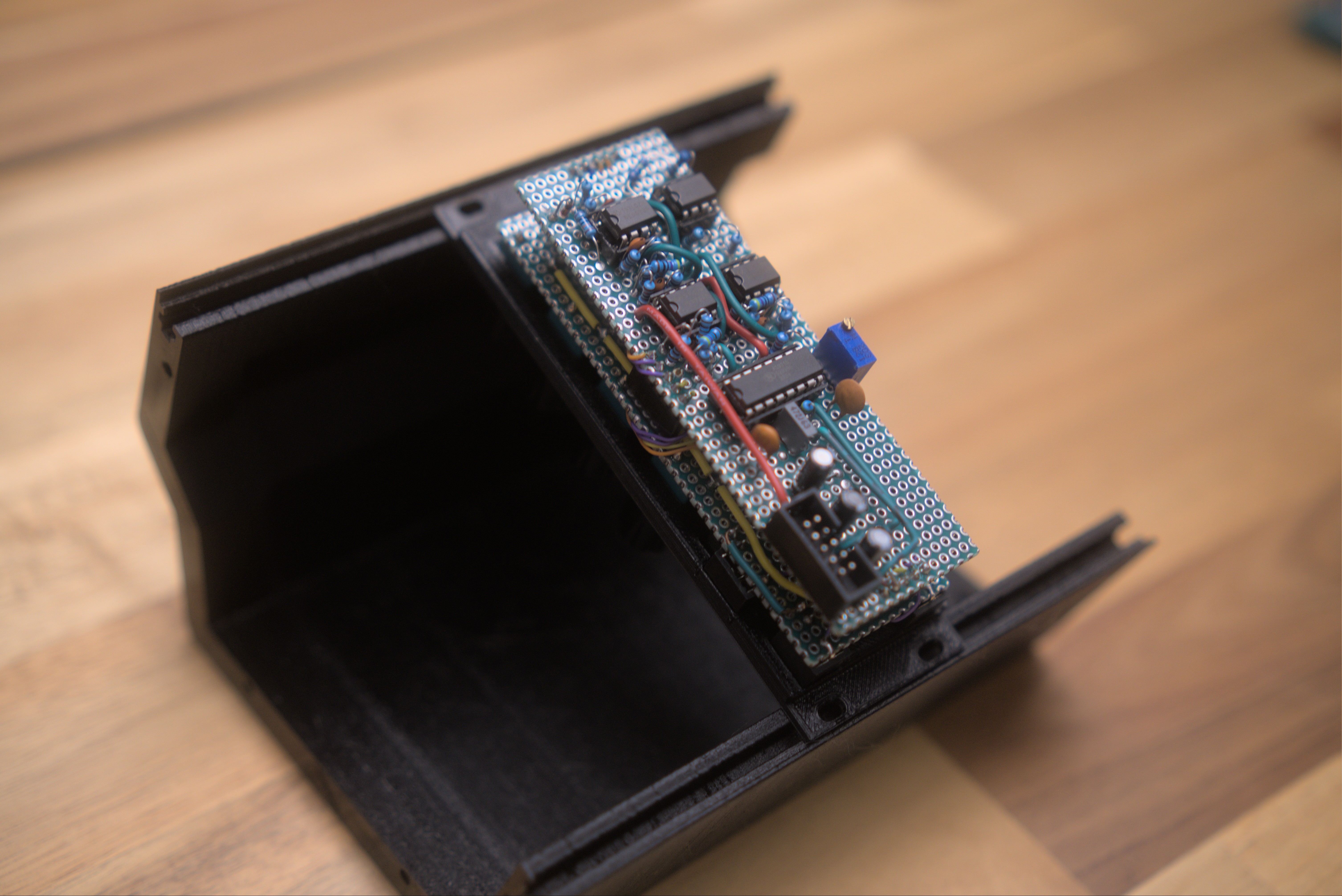
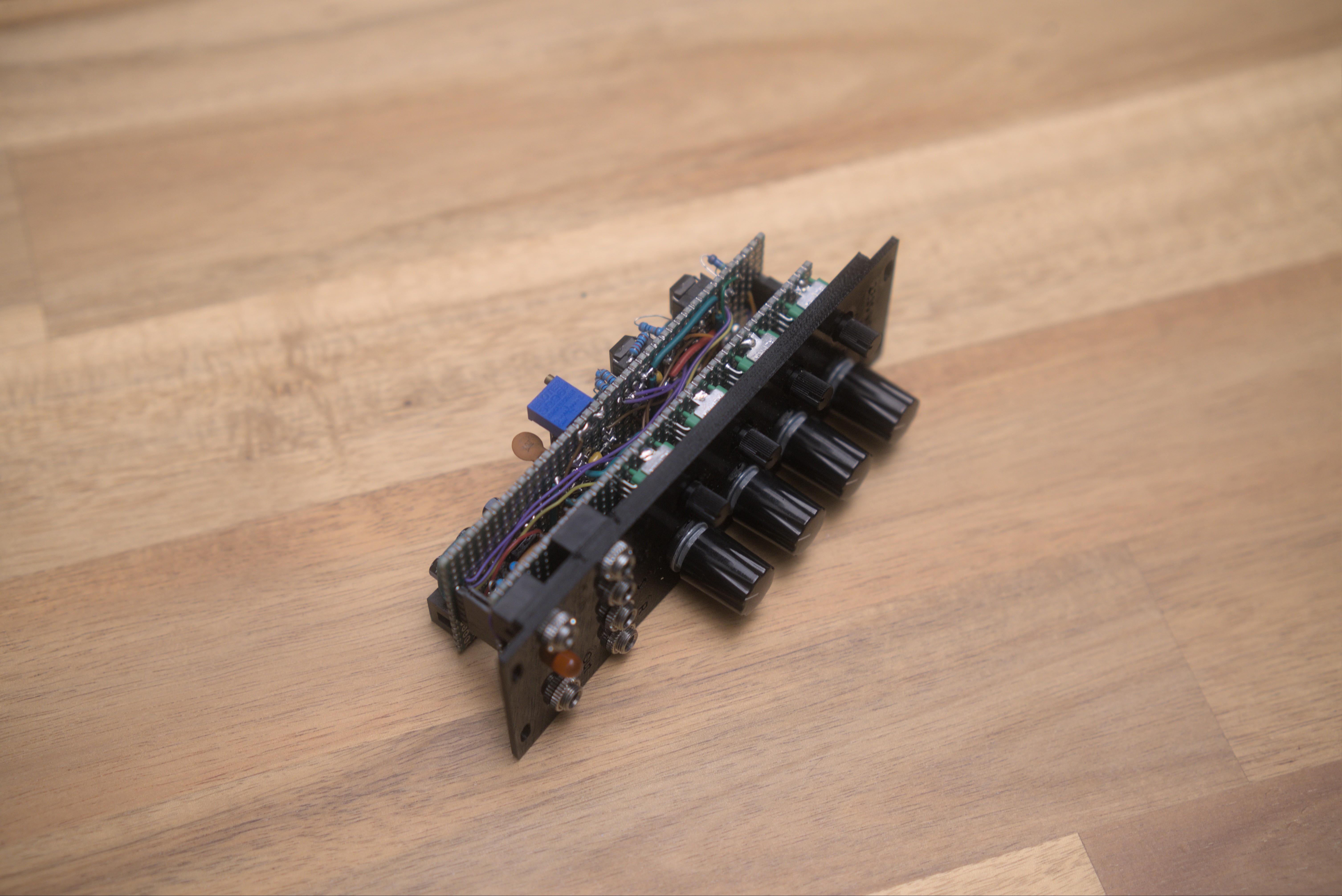
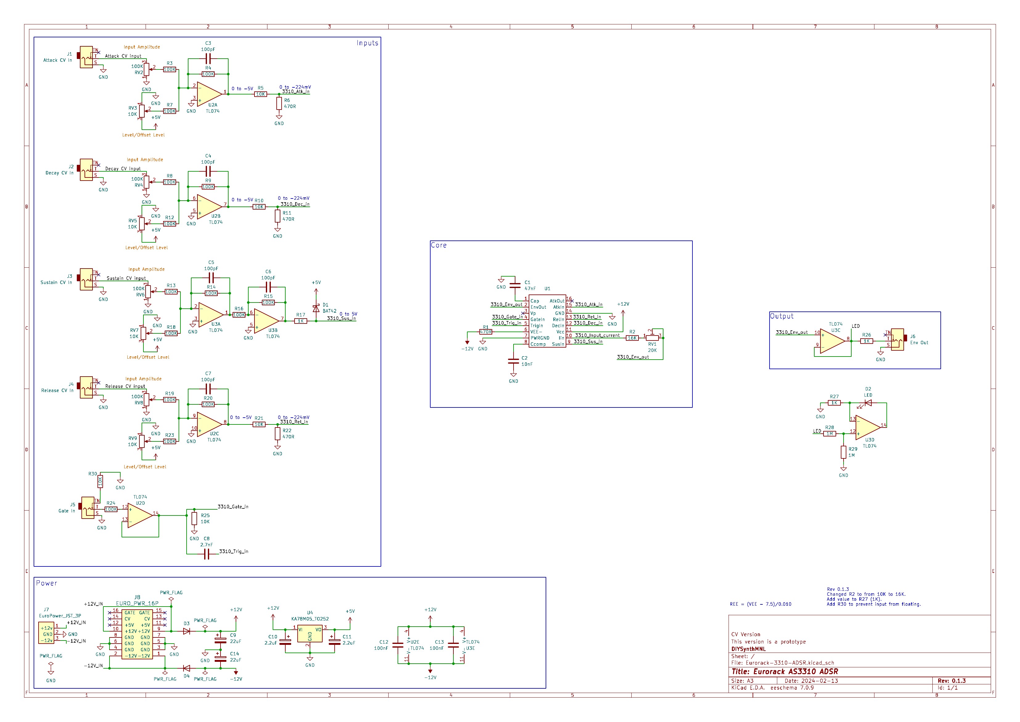
Design Notes
The Attack, Decay, and Release CV inputs are inverting mixers.
The sustain circuit is a combination of an inverting mixer and an inverting amp with a gain of 1 to invert it back in phase. A schottky diode clamps the positive voltage to +5v.
Check out the falstad circuit simulation here
Schematic
Conclusion
If you’d like to build this module, I have provided a 3D printed front panel file in the repo. I used readily available green perfboard. The components should line up with the perfboard’s holes. The panel was made using benjiaomodular’s europanelmaker.