To jumpstart your PCB design I will list my recommended track widths for module PCBs. If you’re going for another manufacturer, be sure to know their capabilities.
- PCBWAY capabilities https://www.pcbway.com/capabilities.html
Track widths
https://www.reddit.com/r/synthdiy/comments/y1be7v/pcb_design_how_do_you_pick_trace_widths_for_your/
- 0.02” for signal, 0.127mm, or 5 mils
- 0.035” for power, 0.889mm,
- PCBWAY: 4mil minimum, recommends a trace width above 6mils (0.15mm)
Minimum track clearance
- PCBWAY: 4mil minimum, recommended 6mil
Vias
- 0.2mm inner dia, 0.5mm outer dia
- PCBWAY: Min drill size is 0.2mm, max drill is 6.3mm. Any holes greater than 6.3mm or smaller than 0.3mm will be subject to extra charges.
Pads
- For my longer pad footprints I use 2.54mm L * 1.6mm W with a 0.8mm hole
- PCBWAY: Min drill size is 0.2mm, max drill is 6.3mm. Any holes greater than 6.3mm or smaller than 0.3mm will be subject to extra charges.
Text
- PCBWAY: min character width is 0.15mm
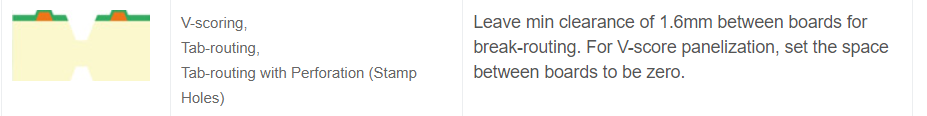
Panelization